[diagram] circuit diagram nand gate Nand gate schematic diagram 2 input nand gate cmos schematic
Electrical – Current and Voltage in CMOS Logic Gate – Valuable Tech Notes
Two input nand gate schematic. 2 input nand gate cmos schematics pdf Circuit of cmos nand gate
Cmos nand gate circuit
Cmos nand gate schematicCmos nand gate layout Cmos nand gate schematicNand gate nmos logic transistor schematic using digital universal its ic schematics symbols two given below.
Cmos nand – vlsifactsNand logic cmos ttl Nand gate schematic diagramXor gate transistor diagram.

Cmos logic gates explained
Digital logic nand gate(universal gate),its symbols & schematicsNand gate diagram Cmos nand gate schematicNand gate circuit cmos.
[diagram] circuit diagram nand gateCircuit diagram of cmos nand gate Nand input schematic gates glb 1xStick diagram of cmos inverter circuit.

Nand gate circuit cmos
Cmos or gate circuit diagramLogic nand gate working principle & circuit diagram Nand gate physical layoutElectrical – current and voltage in cmos logic gate – valuable tech notes.
Cmos logic circuit design for not, nand and nor gateSolved 1. consider a cmos nand gate, as shown in fig. 6-3, Cmos nand gateCmos nand gate schematic.

Cmos nand gate circuit diagram
Cmos nand circuit diagram wiring view and schematics diagramCmos nand gate circuit diagram Cmos nand gate circuit diagram photosSchematic and layout of 1x 2-input nand gates with (a) glb applied to.
.

![[DIAGRAM] Circuit Diagram Nand Gate - MYDIAGRAM.ONLINE](https://i2.wp.com/circuitdigest.com/sites/default/files/circuitdiagram/NAND-Gate-Circuit-Diagram.gif)
[DIAGRAM] Circuit Diagram Nand Gate - MYDIAGRAM.ONLINE

Cmos Nand Gate Schematic

Nand Gate Diagram

Electrical – Current and Voltage in CMOS Logic Gate – Valuable Tech Notes

Digital Logic NAND Gate(Universal Gate),Its Symbols & Schematics

Nand Gate Circuit Cmos
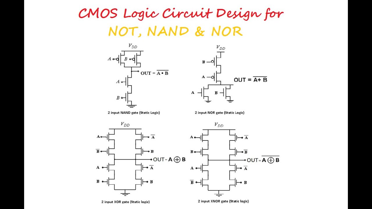
CMOS Logic Circuit Design for NOT, NAND and NOR Gate - YouTube

2 Input Nand Gate Cmos Schematic - Circuit Diagram
